APPLICATIONS:
Raman Spectrometer
Raman Spectrometer
Manufacturing and Packaging of Semiconductors
The capacity of the Raman microspectroscopy has been well exploited in the field of semiconducting materials. It can detect with no sample preparation microinhomogeneities in integrated circuits, defects in both optoelectronic, microelectronic and sensor devices, that are of special technological interest in connection with their possible influence on the device performance. The method also permits quantitative and nondestructive microanalysis of structures and electrical properties in semiconductors. These mainly include damage induced by ion implantation, strains in heterostructures, measurements of crystallographic orientations, polycrystalline grains size and free carriers concentration.
Applications:
Material purity
Defect analysis
Alloy composition
Superlattice structure
Pollutant identification
Semiconductor heterostructure
Doping effect of heterojunction
Characteristic factors of intrinsic stress & strain
Photoluminescence microscopic analysis of material purity
Example: Photoresist (residue) detection
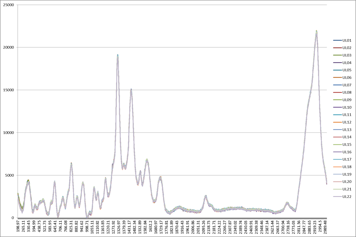
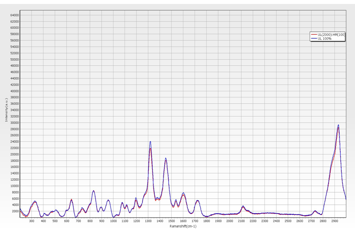
For sample group A: PR_UL photoresist with the same composition and concentration. The test is performed, and the highly consistent results can be obtained by observing the Raman spectrum.
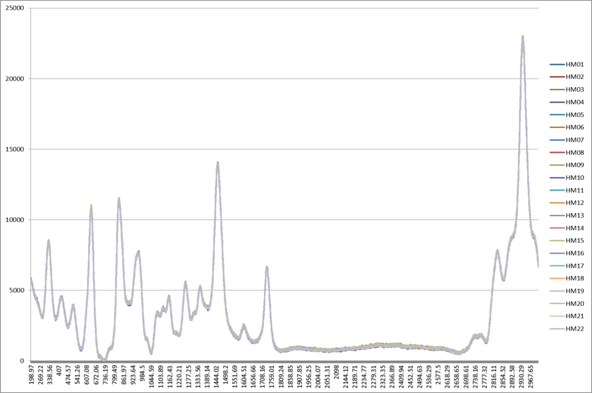
For sample group B: PR_HM photoresist with the same composition and concentration. The test is performed, and the highly consistent results can be obtained by observing the Raman spectrum.
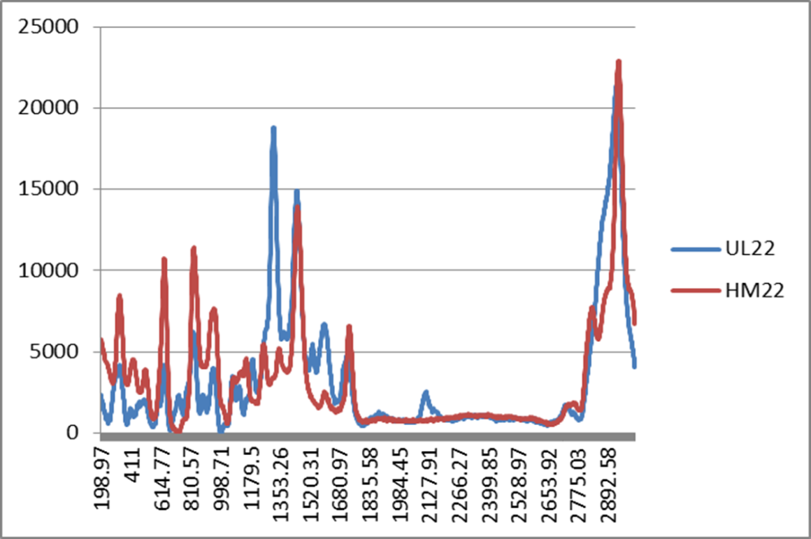
Sample group A & B, judging and distinguishing two photoresists with different components.
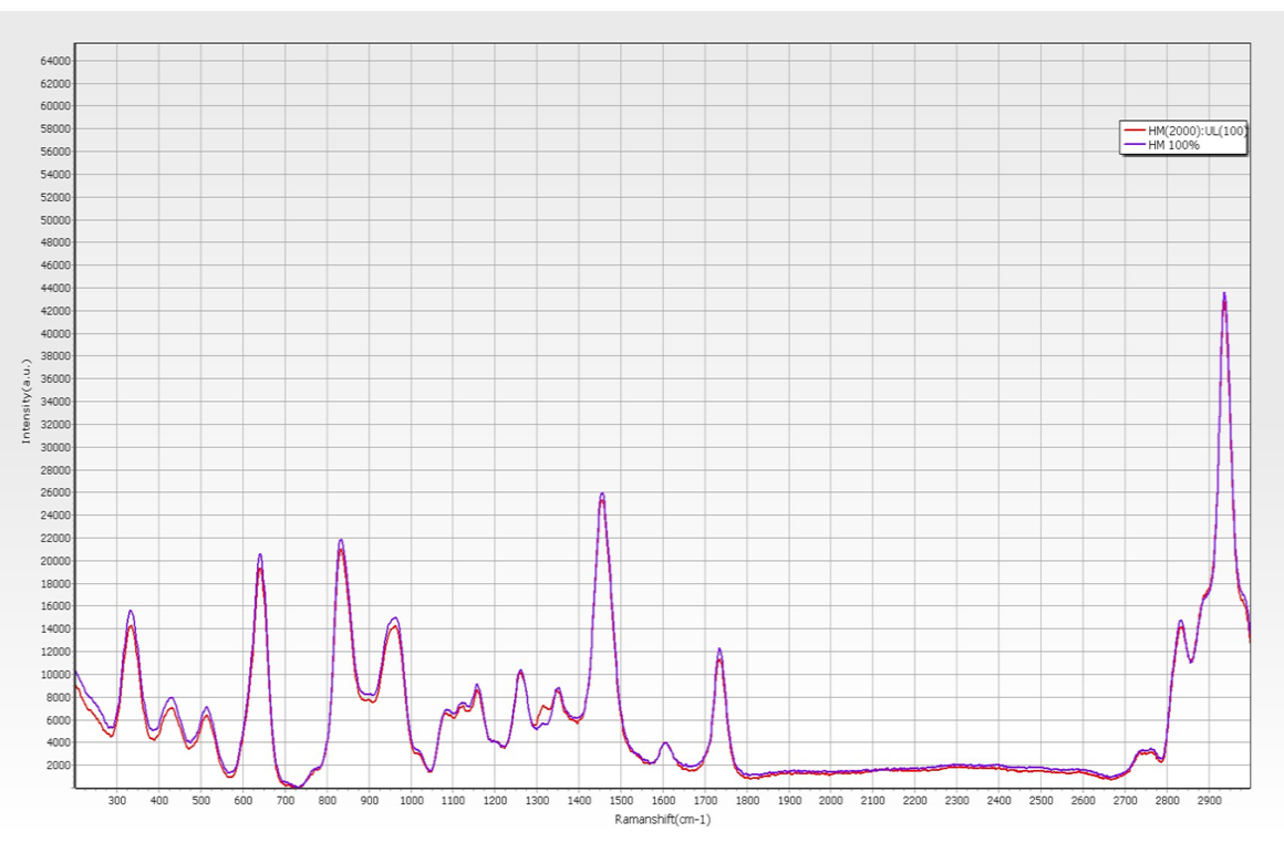
With the Raman analyzer, you can easily see if there is any contamination in the photoresist: UL+5% HM vs. 100% UL.
With the Raman analyzer, you can easily see if there is any contamination in the photoresist: HM+5% UL vs. 100% HM.